Small outline integrated circuit
A small-outline integrated circuit (SOIC) is an integrated circuit (IC) package which occupies an area about 30 - 50% less than an equivalent DIP, with a typical thickness that is 70% less. They are generally available in the same pinouts as their counterpart DIP ICs. The convention for naming the package is 'SOIC' or sometimes just 'SO' followed by the number of pins. For example, a 14-pin 4011 would be housed in an SOIC-14 or SO-14 package.
JEDEC and EIAJ standards
'SOIC' actually refers to at least two different package standards. The EIAJ SOIC body is approximately 5.3mm (0.209") wide while the JEDEC SOIC body is approximately 3.8mm (0.150") wide. Otherwise the packages are very similar.
Note that because of this, SOIC is not specific enough of a term to describe parts which are interchangeable. Many electronic retailers will list parts in either package as "SOIC" whether they are referring to the JEDEC or EIAJ standards. The wider EIAJ packages are more common with higher pin count ICs, but there is no guarantee that an SOIC package with any number of pins will be either one or the other.
General package characteristics
This package is shorter and narrower than DIPs, the side-to-side pitch being 6 mm for an SOIC-14 (from lead tip to lead tip) and the body width being 3.9 mm. These dimensions differ depending on the SOIC in question, and there are several variants. This package has "gull wing" leads protruding from the two long sides and a lead spacing of 0.050 inches.
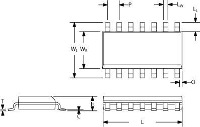
The picture below shows the general shape of an SOIC, with major dimensions. The values of these dimensions (in mm) for common SOICs is shown in the table.
| Package | WB | WL | H | C | L | P | LL | T | LW | O |
|---|---|---|---|---|---|---|---|---|---|---|
| SOIC-8 | 4.0 (3.8) | 6.2 (5.8) | 1.75 | 0.25 (0.10) | 5.0 (4.8) | 1.27 | .41 (1.04) | .19 (.25) | .51 (.33) | .33 |
| SOIC-14 | 3.9 | 5.8-6.2 | 1.72 | 0.10-0.25 | 8.55-8.75 | 1.27 | 1.05 | 0.19-0.25 | 0.39-0.46 | 0.3-0.7 |
| SOIC-16 | 3.9 | 5.8-6.2 | 1.72 | 0.10-0.25 | 9.9-10 | 1.27 | 1.05 | 0.19-0.25 | 0.39-0.46 | 0.3-0.7 |
| SOIC-16 | 7.5 | 10.00-10.65 | 2.65 | 0.10-0.30 | 10.1-10.5 | 1.27 | 1.4 | 0.23-0.32 | 0.38-0.40 | 0.4-0.9 |
SOP
After SOIC came a family of smaller form factors, Small Outline Package (SOP), with a pin spacing of 0.65 mm:
- Plastic Small-Outline Package (PSOP)
- Thin Small-Outline Package (TSOP)
- Shrink Small-Outline Package (SSOP)
- Thin-Shrink Small Outline Package (TSSOP)
The ICs on DRAM memory modules were usually TSOPs until they were replaced by ball grid array (BGA).
